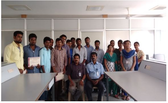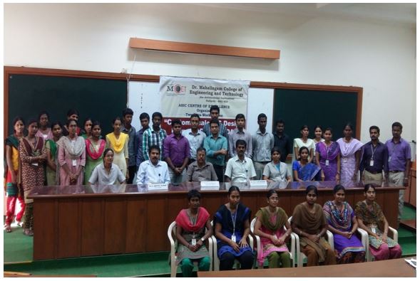
ASIC CENTRE OF EXCELLENCE
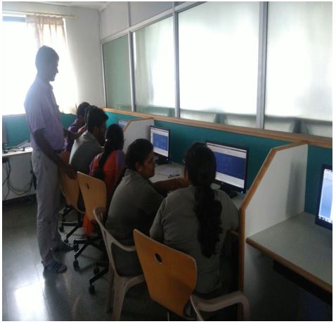
ASIC Centre of Excellence was established in Collaboration with Cadence Design Systems, Ireland in the year 2013, with the primary objective of imparting skill set to students in custom IC and Reconfigurable FPGA designs on par with present semiconductor industry needs.
Objectives of the partnership
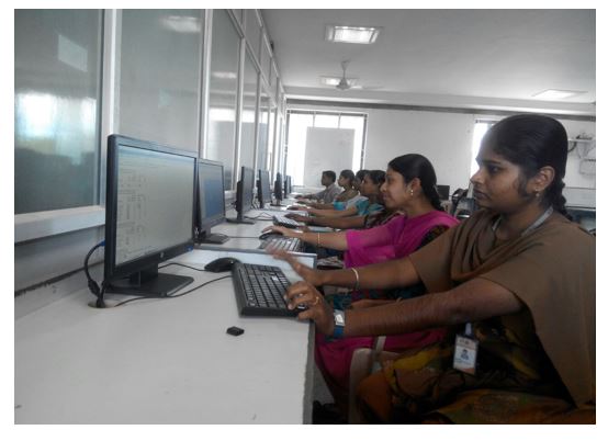
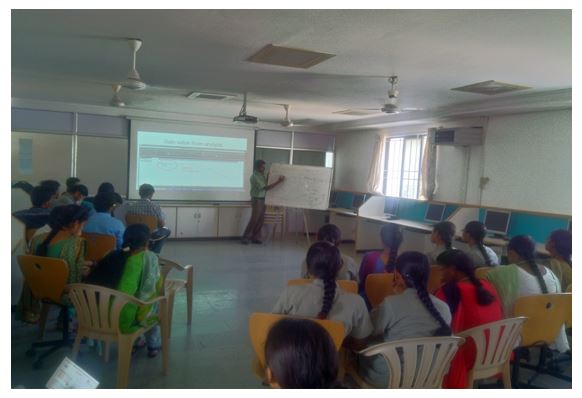
1.Opportunity to engage with the Industry on a regular basis to understand their needs and constantly upgrade the hands-on training offered in Physical Design using Cadence EDA Suite and Reconfigurable FPGA design for signal and image processing applications.
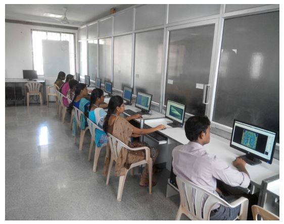
2.Opportunity to upgrade the infrastructure in VLSI and Embedded System Design relevant to semiconductor industry needs.
3.Opportunity to collaborate with the industry for research programs, projects, student internships and IC fabrication.
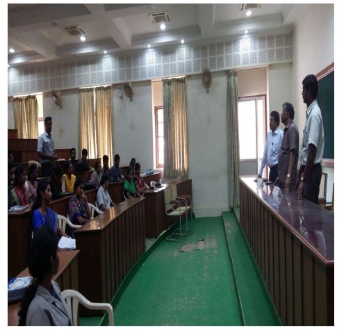
4.To offer Faculty Development Programs(FDPs), hands-on training and workshops in Custom IC and Reconfigurable VLSI architecture designs for teaching staff and students.